Virginia Tech engineers develop new process for creating micro- and nanostructures on 3-D materials

A process for creating micro- and nanostructures on 3-D objects holds great promise to usher in new nano-enabled applications in advanced materials and biotechnology.
The work, published in the journal Nanoscale in July, drastically reduces costs while speeding the production process by four to six orders of magnitude, compared to current state of the art techniques, according to Virginia Tech mechanical engineering doctoral student Zhou Ye; his advisor, Associate Professor Bahareh Behkam; and their collaborator, Associate Professor Amrinder Nain.
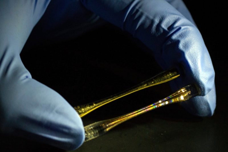
Their process, called Spun-Wrapped Aligned Nanofiber (SWAN) lithography, can fabricate micro- and nanostructures on the entire surface of any 3-D object by applying polymer fiber that is about 500 times smaller than the diameter of human hair over an object, followed by etching areas of the object not covered by the fiber and then removing the fiber itself, thus resulting in a nanotextured gold surface.
Gold film is widely used in biosensing applications due to its nonreactive and conductive nature. With SWAN lithography’s ability to pattern the entire 3-D object independent of curvature, the sensing area along with the signal-to-noise ratio are substantially increased. The process works on all 3-D objects irrespective of their geometry, thereby overcoming a major limitation of current methods, which work only on simple geometries (such as cylindrical objects) or flat surfaces.
In addition to its ability to pattern complex-shaped objects, SWAN lithography also has three additional characteristics that, in the words of Behkam, “make the potential for the process, expansive. The first is that SWAN lithography can be applied to a wide variety of object shapes of varying curvatures, and be done at both micro- and nanoscales, something electron beam lithography (EBL) and focused ion beam milling (FIB) can’t do,” Behkam said. “Second, we have reduced the costs considerably; and finally, the time it takes to texturize an object is orders of magnitude faster compared to other methods.”
Behkam contends the current commercially available systems for creating nanostructures typically take 10,000 to 1 million times as long. That means what SWAN lithography can do in one minute, the others would spend 166 hours or 694 days to accomplish.
“Really, it allows us to explore a large variety of application areas. We are especially interested in health care-related technologies,” Behkam said. “We are working to engineer nanocomponents that work with biologic components. For example, in implantable medical devices, microbial infections are not only associated with increased mortality but are also significant contributors to the emergence of antibiotic resistance traits. With increased life expectancy, we are likely to see an increase in the use of short- and long-term implantable biomedical devices. This represents a growing unmet medical need to counter microbial biofilm-associated infections. Current treatment for biofilm-associated infections typically involve a combination of surgical replacement of the implant and long-term antibiotic therapy, which incurs high health-care costs and remains controversial because compelling evidence of their effectiveness is lacking. SWAN lithography enables engineering of micro/nano-scale topological cues on the surface of medical implants to mitigate biofilm formation, allowing a far-superior function and safety.”
In addition to medical applications, the SWAN lithography process also allows functionality to be built into other products, including nanosensors for photonic and plasmonic applications.
Currently, Behkam and her team are speaking with industry to further develop the patent-pending technology and bring it to the next step for wide-scale use in everything from camera lenses and aircraft wings, to ship hulls, solar panels, and biomedical devices and implants.
Written by Rosaire Bushey


